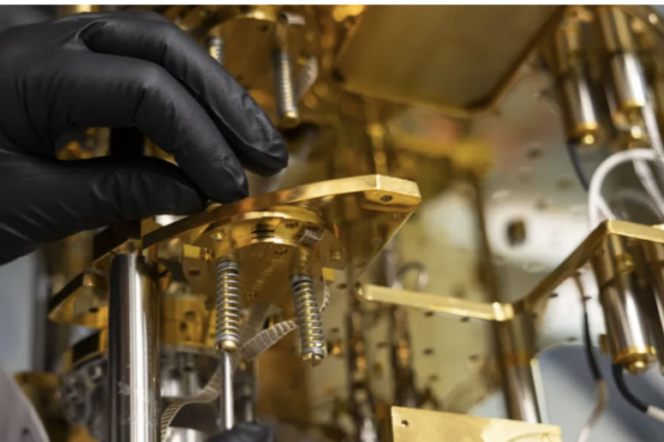
Two-dimensional materials have spent more than a decade in a state of suspended anticipation. In laboratories, they have looked like the next act in electronics, photonics and sensing: atomically thin conductors, semiconductors and insulators with the potential to shrink devices further, cut power, and enable entirely new stacks of functionality. In manufacturing, they have remained stubbornly awkward. The obstacle has not been the elegance of the physics. It has been the duller, harder question of process integration: how do you move exquisitely thin materials from growth substrates into the contamination-sensitive, yield-driven routines of semiconductor production without ruining the very properties that made them interesting in the first place?
That is the problem In2great Materials, a Swedish deep tech spin-out from KTH Royal Institute of Technology, has set out to solve. The company does not present itself as a maker of futuristic gadgets. It says, more plainly, that it brings “2D materials into semiconductor foundries”, and that its key advantage is the use of “only established equipment and materials” already available in semiconductor fabs. KTH, which lists In2great Materials AB among its spin-offs, describes it as a company whose technology brings atomically thin materials into foundries and could advance sensing, photonics and electronics. This is not the language of moonshots. It is the language of process adoption.
That distinction is crucial. Semiconductor manufacturing is not impressed by theoretical promise alone. It rewards technologies that can be inserted into existing lines with tolerable risk, known materials, compatible thermal budgets, acceptable contamination profiles and a plausible route to scale. In this respect, In2great is pursuing one of the least glamorous and most consequential plays available in advanced materials. It is not trying to outshine silicon with a single breathtaking device. It is trying to solve the plumbing problem that keeps new materials out of production. If that sounds prosaic, it is worth remembering that entire waves of semiconductor innovation have depended less on discovering a remarkable property than on finding a repeatable way to integrate it.
The company’s scientific base is unusually visible. Its most important public foundation remains the 2021 Nature Communications paper “Large-area integration of two-dimensional materials and their heterostructures by wafer bonding”, led by Arne Quellmalz and colleagues from KTH and partner institutions in Germany. The paper states the industrial challenge without adornment: integrating 2D materials into semiconductor manufacturing lines is essential if their properties are ever to matter commercially, yet “current approaches are not compatible with high-volume manufacturing on wafer level”. The significance of that sentence lies in what it leaves unsaid. For years, the 2D-materials field produced elegant experiments, striking device demonstrations and an expanding library of materials, but never managed to make transfer and integration look routine to a fab engineer. In2great emerged from research that explicitly set out to change that.
To see why that matters, it helps to look closely at the transfer problem itself. High-quality 2D materials such as graphene and MoS2 are typically synthesised at temperatures too high for already processed silicon electronics. That means they cannot simply be grown where they are ultimately needed. Instead, they must be transferred from a dedicated growth substrate to a target wafer that may already contain circuits, photonic structures or MEMS features. According to the 2021 Nature Communications paper that underpins In2great’s platform, this is the decisive industrial bottleneck: existing transfer methods had not delivered a route that was both compatible with high-volume wafer-level manufacturing and capable of preserving material quality well enough for demanding devices.
Traditional wet-transfer methods typically rely on polymer support layers such as PMMA and involve lifting the atomically thin film from a liquid surface and redepositing it onto a new substrate. Those processes are widely used in research, but they can leave polymer residues, introduce wrinkles and strain, and degrade transport properties. Dry-transfer approaches avoid some wet-processing problems, yet they have often brought their own issues, including cracks, contamination and uneven mechanical deformation. The KTH-led paper reviews these shortcomings directly and concludes that neither class of method had become properly compatible with industrial semiconductor routines.
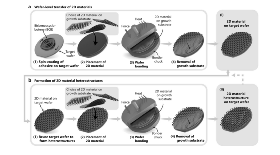
In2great’s answer is to treat transfer as a wafer-bonding problem rather than a manual handling problem. In the published method, a target wafer is coated with a thermosetting adhesive layer of bisbenzocyclobutene, or BCB, and soft-baked. The donor substrate carrying the 2D material is then placed on top, with the material facing the adhesive. The full stack is loaded into a commercial wafer bonder, where heat and controlled force lower the viscosity of the BCB so that it moulds to the topography of the donor substrate and the 2D layer. After bonding, the donor substrate is removed, leaving the 2D material on the target wafer. Because the BCB is only partly cross-linked under carefully chosen conditions, the process can be repeated, allowing multiple 2D layers to be stacked into heterostructures.
The industrial significance lies in what the process avoids. It avoids manual handling of released films. It avoids sacrificial polymer carrier layers at the key upper interfaces of heterostructures. And, crucially, it uses materials, tools and process logic that semiconductor manufacturers already recognise. The Nature Communications paper explicitly says the method relies only on equipment, processes and materials “readily available in large-scale semiconductor production lines”. In2great’s website now makes the same point in commercial language, stressing that the use of existing fab tools is a prerequisite for adoption in a “price- and risk-sensitive” industry.
That phrase, “a crucial prerequisite”, is the key to the whole company. The semiconductor sector is famously conservative for reasons that are entirely rational. Novelty that cannot be qualified, replicated and costed is simply another way of saying risk. A process that uses a known adhesive, standard bonding tools and familiar wafer-scale handling starts from a much better place than one that depends on operator skill, fragile floating films or bespoke intermediates. In2great is therefore not just offering better transfer. It is pitching a lower-friction path to adoption, which is often the more valuable thing. The most disruptive part of the platform may not be the materials at all, but the decision to take the foundry’s habits seriously.
There is something almost unfashionable about that strategy. The rhetoric around deep tech often favours technologies that appear to overthrow incumbents in one dramatic leap. In2great’s proposition is subtler and, for that reason, arguably more credible. Instead of asking manufacturers to abandon the industrial grammar of wafer bonding, dielectrics, thermal budgets and scaled handling, it asks whether atomically thin materials can be folded into those routines. KTH’s own summary of the underlying research made the point in plain terms: the solution lies in “the existing toolkits of semiconductor manufacturing”. For an enabling technology, that is exactly the right argument to make.
The scientific results in the Nature Communications paper are strong enough to explain why that argument has gained traction. The researchers demonstrated transfer of CVD graphene from copper foils to 100 mm silicon wafers, transfer and stacking of graphene with hexagonal boron nitride, formation of double-layer graphene by repeated transfer, and transfer of multilayer MoS2 onto 100 mm wafers. They also fabricated encapsulated field-effect graphene devices after transfer and reported charge-carrier mobilities up to 4520 cm² V⁻¹ s⁻¹. On transferred graphene resting on BCB, van der Pauw measurements yielded average mobility of 2800 ± 100 cm² V⁻¹ s⁻¹. Non-contact terahertz measurements indicated uniform graphene coverage over the full wafer. The paper’s claim was not that these were world-record numbers. It was that they were achieved in a wafer-level process built around industrially legible steps.
That distinction matters more than the headlines suggest. In semiconductor manufacturing, dazzling peak performance in a few handcrafted devices rarely matters as much as acceptable performance across a repeatable process. The authors underline this, noting that meaningful comparisons depend heavily on the starting quality of the graphene itself. Their real point is that adhesive wafer bonding can preserve material quality well enough to support conventional device fabrication after transfer. In the top-gated field-effect devices, the graphene survived multiple lithography steps, atomic-layer deposition of Al2O3, metal depositions and etching without catastrophic loss of function. This is precisely the sort of evidence process engineers look for when they ask whether a materials trick can survive contact with the rest of the line.
The graphene results are only part of the story. In many ways, the more important proof is that the method appears generic. The team also transferred multilayer MoS2 from SiO2/Si growth chips to 100 mm target wafers and used Raman and photoluminescence spectroscopy to assess the films before and after transfer. The strain-sensitive E^1_2g Raman mode showed no detectable shift within the accuracy of the setup, suggesting that the process did not introduce major new strain. They then built MoS2/graphene heterostructures through consecutive transfers and confirmed the integrity of both materials. This matters because a transfer method that works only for one material may still be useful, but a method that can accommodate multiple layered materials and their heterostructures becomes something closer to a platform. In2great’s website conspicuously avoids overfocusing on graphene alone, instead talking about “2D materials” as a class. The science gives that generalisation some credibility.
There is also a subtler technical strength in the bonding approach. The paper argues that because the BCB becomes viscous during bonding and moulds to the donor substrate topography, the transferred layer can retain much of the shape it had on the growth substrate rather than being forced into a new geometry that generates wrinkles or excess strain. The authors hypothesise that this helps preserve the mechanical state of the 2D material. In a field where microscopic wrinkles, random strain fluctuations and contamination residues can ruin transport properties, that is not a cosmetic advantage. It is a process insight. At the same time, the paper is careful enough to note a trade-off: if the donor substrate has pronounced topography, that relief can be replicated into the bonded structure and may later complicate very high-resolution lithography. This is exactly the kind of caveat that deserves attention because it signals a research team that is thinking like process engineers rather than evangelists.
The transition from published research to company formation appears unusually coherent. KTH’s spin-off page identifies In2great Materials AB as founded in 2022. The company says it was founded by KTH researchers who have worked on 2D-material devices for photonics and sensing, as well as MEMS integration strategies, for more than ten years. Corporate registry data collated by allabolag.se show the company legally registered in September 2021, with business activities including development, sale and licensing of products and technology in materials, particularly for microelectronics. The same source reports 2024 turnover of SEK 4.891 million and five employees. Those are still small-company numbers, but they indicate a real operating entity rather than a dormant patent vehicle. In semiconductor enabling technology, modest revenue at this stage can be a sign of early process-development work, public funding and contract activity rather than a lack of seriousness.
The intellectual-property trail reinforces that continuity. The Nature Communications paper discloses that several of the academic authors are co-inventors on a patent application covering the transfer method. Public patent records show the related PCT publication WO2020152358A1, “Method of material transfer”, and a granted US patent, US11504959B2. The patent abstract closely mirrors the scientific paper: an atomically thin layer is transferred by providing donor and target substrates, disposing an adhesion layer, bonding the stack and removing the donor substrate. Patents do not guarantee market power, particularly in process technology where tacit know-how often matters more than formal claims, but they do suggest that the academic team understood early that scalable integration would be a protectable asset rather than merely a publishable result.
If the company’s formation shows organisational continuity, the Vinnova funding trail shows translational intent. One Vinnova-backed project, running from April 2022 to March 2025 with nearly SEK 5 million in funding, stated that it matured In2great’s technology “to a level suitable for deployment in semiconductor foundries” and focused on demonstrators, product portfolio and market-fit validation with industrial users. A second project, running from December 2023 to June 2026, is more pointed still. It says the company will validate its “disruptive technology” in an industrial setting, work with a “product-owning customer”, establish a value chain for mass production and conduct a “full pre-production run”. Another, shorter Vinnova project reported that In2great had fabricated prototypes of novel transistors with very high-quality 2D materials and that the work helped secure engagement with “a large semiconductor manufacturer”. A 2024 to 2026 programme then set out to build a Swedish value chain for high-volume graphene-based sensors integrated with CMOS electronics, explicitly involving a semiconductor and MEMS foundry and a sensor supplier.
These project descriptions should be handled with care. Vinnova notes that the text is supplied by project members and not reviewed by editors. Even so, the chronology is telling. The company did not stop at publishing wafer-scale transfer results. It moved towards demonstrators, industrial dialogue, pre-production language and value-chain construction. That is the normal sequence for a process startup that intends to survive the brutal transition from academic proof to foundry relevance. It also suggests that In2great understands where first markets are likely to appear. The most concrete public industrial language so far concerns sensors, especially graphene-based or microelectronic sensors, rather than attempts to replace front-end CMOS logic. That is not a retreat. It is a realistic reading of where 2D materials are most likely to gain traction first.
That focus on sensors is more important than it may first seem. In public discussion, the phrase “next-generation electronics” can subtly imply a race to displace silicon in the core logic stack. In practice, 2D materials are more likely to establish themselves first where they offer added functionality rather than full substitution. Graphene’s high carrier mobility, optical absorption and sensitivity to environmental perturbations make it attractive for photodetectors, Hall sensors and chemical sensing. Transition-metal dichalcogenides such as MoS2 add semiconducting behaviour and promising optoelectronic characteristics. A foundry-compatible transfer technology is therefore especially valuable in sectors where hybrid integration matters: putting atomically thin active materials on top of mature silicon, rather than asking the industry to abandon silicon’s manufacturing base.
This is where In2great begins to look less like a conventional startup and more like an enabling layer in a broader ecosystem. Its value proposition only fully makes sense when seen alongside the industrial architecture of contemporary semiconductors. Foundries do not simply manufacture chips. They operationalise standards, qualification regimes, toolsets, test infrastructures and complex supplier relationships. A new materials company that expects all of that to bend around a laboratory technique is asking too much. A company that can make its process legible to foundries, integrate with MEMS and sensor lines, and fit within existing supply chains is making the far more difficult but far more serious move. This is why Vinnova’s repeated language about value chains, product-owning customers and pre-production runs matters. It suggests the company understands that no transfer technology is commercial until it fits a real chain of manufacturing responsibility.
The broader policy backdrop helps explain why this kind of company may matter more now than it would have a few years ago. The European Chips Act, which entered into force in September 2023, aims to strengthen the Union’s semiconductor ecosystem, reduce strategic dependencies and build greater capacity in research, design, manufacturing, packaging and supply resilience. Europe’s own policy language stresses the need to bridge research and industrial production, including through pilot lines and mechanisms that support “first-of-a-kind” facilities and open foundries. None of this is specifically about 2D materials, and In2great should not be inflated into a geopolitical symbol. But the company does sit neatly within a larger European effort to close the gap between excellent research and usable manufacturing capability. If Europe wants sovereignty not only in fab capacity but in the enabling technologies that allow new materials to be industrialised, then process-integration companies like this one become more than academic curiosities.
It is also worth noting that Europe’s semiconductor strengths have often lain less in sheer manufacturing scale than in equipment, advanced materials, specialised devices, research excellence and industrial end markets such as automotive, industrial systems and instrumentation. That ecosystem is not a natural habitat for every kind of chip startup, but it can be fertile ground for companies whose value lies in adding differentiated functions to mature platforms. In2great’s emphasis on foundry readiness, sensor integration and existing infrastructure fits that pattern. It is not trying to win by brute scale. It is trying to become the connective tissue between frontier materials research and those parts of the semiconductor economy where Europe remains especially strong.
Still, the cautions are real and should not be buried under the narrative. Public evidence shows convincing science, a credible academic lineage, protected IP and grant-backed commercialisation. It does not yet show named foundry deployments, published reliability data under product-relevant stress conditions, or public results at 200 mm and 300 mm scale. The flagship Nature Communications paper demonstrates 100 mm wafer integration. That is significant, especially in MEMS, photonics and some speciality processes, but it is not the same thing as mainstream high-volume CMOS production. Likewise, Vinnova’s language about industrial validation and pre-production is encouraging but still one step removed from publicly documented product integration by major customers. A forensic reading lands somewhere between admiration and reserve. The platform looks important. The final proof of industrial adoption remains ahead.
There are also specific technical questions that remain unresolved in public. One concerns contamination. The 2021 paper improves dramatically on polymer-supported wet transfer by avoiding carrier-layer contact at key heterostructure interfaces, but it openly acknowledges that copper residuals and copper-etchant residues remain potential contaminants when graphene is transferred from copper foils. In a paper, that is admirable candour. In a fab, it is a process-control challenge with real implications for qualification. Another question concerns topography and lithography. The method’s strength lies partly in preserving the donor substrate’s surface relief, but that very relief may become problematic when later fabrication steps demand tight planarity or high-resolution patterning. A third issue is stack control. The researchers demonstrated repeated transfer and stacked layers, but not deterministic twist-angle alignment of the sort that some van der Waals physics applications require. None of these gaps invalidates the platform. All of them matter when judging how far it has to go.
Wafer diameter is another obvious and unresolved commercial question. Public data from the Nature Communications paper focus on 100 mm wafers. That is already meaningful in photonics, research-scale process lines and parts of the MEMS world, yet the broader semiconductor ecosystem increasingly lives at larger diameters. Scaling a transfer technology is never only a matter of making a bigger substrate. It means managing edge effects, force distribution, topography, metrology throughput, and defectivity over a larger area. It also means proving that the economics remain sensible as the process moves closer to the expectations of mainstream volume manufacturing. Publicly available evidence does not yet show that full step.
The same caution applies to the back-end-of-line claim. The science behind In2great’s platform is clearly directed at BEOL compatibility, and the 2021 paper explicitly states that the method is suited for integrating 2D materials on top of integrated circuits. Supplementary demonstrations showed features such as cavities and pre-existing contacts in the adhesive layer. More recent public-facing material from Quellmalz and In2great describes the platform as foundry ready, compatible with back-end-of-line processes, and “largely independent of recipient wafer topography and surface properties”. That may well be true in practice, but the public record still contains more scientific demonstration than named foundry case studies. For a journalist, that is the line to hold. The company has earned interest. It has not yet earned a verdict of inevitability.
There is also the business-model question, which remains mostly implicit in public materials. Process startups in semiconductors can license, co-develop, provide specialised services, build their own pilot manufacturing, or embed themselves as indispensable partners in customer qualification cycles. In2great’s website and funded-project descriptions point to a mix of proprietary process technology, industrial collaboration and value-chain building, but they do not publicly spell out the eventual model in detail. That is not unusual at this stage. Still, it matters because the commercial moat of a transfer technology does not rest on patents alone. It depends on know-how, customer integration, qualification data, and the degree to which the process becomes the lowest-friction route for manufacturers to adopt 2D materials without redesigning their entire production logic.
Yet even with those caveats, there is a strong case that In2great represents one of the more interesting Scandinavian deep tech stories in semiconductor enabling technology. The company is grounded in peer-reviewed work of high quality, and that work speaks directly to the industrial pain point rather than merely to laboratory novelty. KTH’s publication record places the 2021 Nature Communications paper within a broader line of work on wafer-scale transfer, photonic integration and 2D devices. Quellmalz’s doctoral thesis frames the transfer method as a route for integrating 2D materials at the back end of semiconductor foundries. The continuity from thesis to publication to patent to company to Vinnova-backed industrial validation is unusually clean. In a field crowded with futuristic claims, that continuity is itself a signal.
The deeper significance of In2great may therefore lie in what it reveals about how advanced materials actually enter industry. Breakthroughs are often narrated as devices: a new transistor, a new detector, a new sensor. The harder truth is that before any of those devices can become commercially meaningful, someone has to solve the uncelebrated sequence of transfer, bonding, metrology, cleaning, alignment, thermal management and yield control. These are not glamorous tasks. They are, however, the tasks on which industrial reality turns. A startup that can solve them becomes disproportionately important because it determines which classes of research ever escape the paper stage. From that perspective, In2great is not merely commercialising a transfer trick. It is attempting to build missing infrastructure for the 2D-materials economy.
In the end, In2great Materials looks important not because it promises a science-fiction future, but because it addresses the most unromantic part of real technological change. New materials do not become industries when they inspire the most papers. They become industries when someone figures out how to move them, bond them, clean them, stack them, pattern them and qualify them within the disciplines of manufacturing. That is the ground on which this company is operating. Its progress so far suggests that the long-stated problem of 2D materials was never only about discovering great properties. It was about making those properties manufacturable.
In2great has not solved that problem for all time. But it has done something more valuable than hype. It has made the problem legible to the fab.
Article based on:
- In2great Materials describes itself as bringing 2D materials into semiconductor foundries using only established equipment and materials, while KTH lists it as a 2022 spin-off from the university.
- The primary scientific account is Arne Quellmalz et al., “Large-area integration of two-dimensional materials and their heterostructures by wafer bonding”, Nature Communications 12, 917 (2021), PDF. KTH’s 2021 news coverage quotes Quellmalz on using the existing toolkit of semiconductor manufacturing. [kth.se], (PDF) Large-area integration of two-dimensional materials and their heterostructures by wafer bonding
- The 2021 paper reviews the drawbacks of conventional wet and dry transfer, including contamination, wrinkles, cracks and incompatibility with high-volume wafer-level manufacturing. Similar background appears in the patent. [patents.google.com]
- The adhesive wafer-bonding process, including BCB coating, bonding under heat and force, donor-substrate removal and repeated stacking of heterostructures, is described in detail in the Nature Communications paper and reflected in the patent abstract.
- The scientific paper describes BCB as a mature semiconductor dielectric used in industrial contexts. In2great and Vinnova both stress the use of established tools and materials as central to adoption. [vinnova.se]
- The transfer of graphene, hBN and MoS2, and the reported electrical and spectroscopic results, are all detailed in the 2021 paper.
- The patent lineage is visible through the paper’s competing-interest disclosure and public patent listings for WO2020152358A1 and US11504959B2. [patents.google.com], [patents.google.com], [patentimag…leapis.com]
- Vinnova’s project database documents the company’s staged move from maturing the technology to industrial validation, pre-production language and value-chain building around sensors and CMOS integration.
- The European Chips Act and related policy material provide the relevant background for why enabling semiconductor process technologies matter strategically in Europe today. [digital-st….europa.eu], [digital-st….europa.eu], [eur-lex.europa.eu]