Modern photonics demands components that are not only fast and efficient but also dynamically tuneable. HyCom Core introduces a breakthrough in this domain: an electrically controllable optical device leveraging the Pockels effect (a linear electro-optic effect where the refractive index of a non-centrosymmetric material changes in response to an applied electric field, allowing for precise control of light) to modulate light properties in real time. This innovation promises to reshape optical communication, sensing, and adaptive optics.
Technical Principle
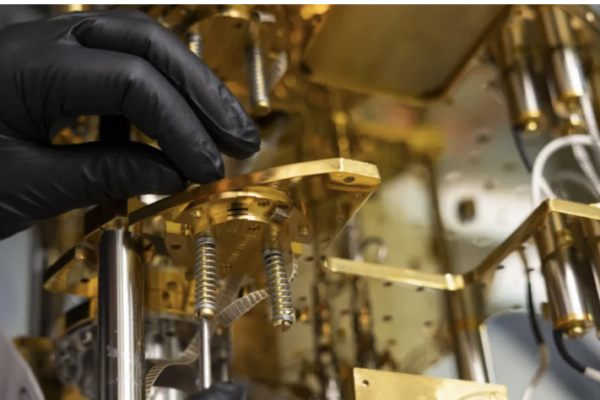
The core of the invention lies in a layered stack of optically transparent materials, including at least one electro-optic material such as lithium niobate. By applying an electric field across the stack, the refractive index can be locally altered, enabling precise control of light propagation at multiple wavelengths. Unlike passive optical components, this device offers active modulation without mechanical movement, reducing latency and improving reliability.
Market Implications
The global photonics market, projected to exceed $900 billion by 2030, is increasingly driven by telecommunication, LiDAR, and quantum computing. Electrically tuneable optics can significantly enhance data transmission rates, reduce energy consumption in optical networks, and enable miniaturized photonic circuits. Companies investing in integrated photonics, especially for 5G/6G infrastructure, stand to benefit from this technology.
Potential Use Cases
- Optical Switches and Modulators: High-speed signal routing in fibre networks.
- Adaptive Lenses: Real-time focus adjustment for cameras and telescopes.
- Quantum Photonics: Precise control of photon states for quantum encryption.
- LiDAR Systems: Dynamic beam steering for autonomous vehicles.
Integration with silicon photonics platforms will be crucial for scalability. Further miniaturization and AI-driven control algorithms could enable self-optimizing optical networks. Research into alternative electro-optic materials may improve efficiency and reduce costs.
Diagram Description:
- Top Layer: Transparent electrode (e.g., indium tin oxide).
- Middle Stack: Alternating layers of electro-optic material (e.g., lithium niobate) and transparent dielectric.
- Bottom Layer: Transparent electrode.
- Electric Field: Arrows indicating applied voltage across electrodes, causing refractive index change in the electro-optic layer.
- Light Path: A horizontal beam passing through the stack, showing modulation.
WO2024213836 CONTROLLABLE OPTICAL DEVICE
Patent Applicants HYCOM CORE Oy and BRIGHTERWAVE Oy with Inventors Janne KONTTINEN & Seppo HONKANEN
See other Photonics innovations from Finland’s photonics innovation centre in Joensuu here at this link