VTT has demonstrated unusually uniform ferroelectric hafnium-zirconium oxide capacitors across a 150-millimetre wafer, an important manufacturing result produced inside Europe’s heavily funded FAMES semiconductor programme. The achievement could help Finland build a credible platform for non-volatile memory and computing-in-memory research. It does not, however, demonstrate a complete memory, an AI accelerator, a hundredfold efficiency gain or a device capable of a trillion useful rewrites. The science is promising. The distance between the science and the headline is the real story.
A careful advance and an exuberant announcement
On 1 July 2026, VTT Technical Research Centre of Finland announced that its ferroelectric memory technology was paving the way for “hyper efficient AI computing”. The announcement contained several of the ingredients now customary in European semiconductor communications: artificial intelligence, energy efficiency, pilot production, technological sovereignty and industrial scalability. It also contained a genuine and peer-reviewed scientific result.
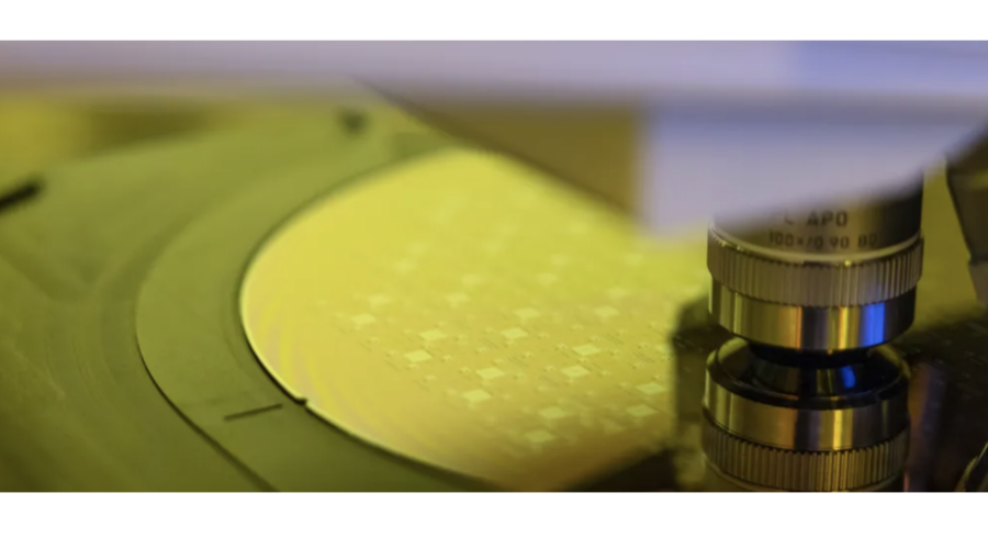
The underlying study, published in Advanced Electronic Materials, reports that VTT fabricated 5.5-nanometre-thick ferroelectric hafnium-oxide/zirconium-oxide structures on 150-millimetre silicon wafers. By depositing the two oxides as a superlattice rather than as the more conventional atomic-scale solid solution, the researchers obtained a higher average remanent-polarisation window and a much narrower distribution across the wafer. The relative standard deviation fell from 7.0 per cent for the solid-solution wafer to 2.2 per cent for the superlattice wafer. Average 2Pr, a measure of the switchable polarisation window, rose from 27.6 to 31.5 microcoulombs per square centimetre.
Those figures matter. Uniformity is not a decorative extra in semiconductor manufacturing. A device that works splendidly in the middle of a wafer but rather loses its convictions near the edge is a scientific specimen, not an industrial platform. VTT’s result suggests that its superlattice structure is less sensitive to variations elsewhere in the fabrication process, including variations in the underlying titanium nitride electrode. That is a useful property when layers are only a few nanometres thick and manufacturing tolerances have become an argument conducted atom by atom.
Yet the paper is not a demonstration of an AI processor, a complete compute-in-memory array or even an integrated memory cell with its required selection and peripheral circuitry. It is principally a materials and process-uniformity study of relatively large metal-insulator-metal capacitors. VTT itself identifies selector integration, substantial footprint reduction, improved yield and greater process repeatability as work still to be done.
That distinction is the organising fact of the story. VTT has solved, or at least substantially mitigated, one problem on a long technical road. The institutional announcement occasionally writes as though the road has already developed a bus service.
What VTT actually built
The devices in the study are capacitors made from a titanium nitride bottom electrode, a 5.5-nanometre HZO switching film and a titanium nitride top electrode. HZO is shorthand for a mixture or layered combination of hafnium oxide and zirconium oxide. In an appropriate crystalline phase, this material can retain one of two polarisation orientations after the applied electric field is removed. These persistent states offer a physical basis for non-volatile memory.
Ferroelectricity describes a switchable internal electric polarisation. An electric field can push the material from one polarisation state to the other, and the state can remain after the field disappears. A conventional capacitor stores charge only while it is maintained electrically. A ferroelectric capacitor can, in principle, encode information in the orientation of its polarisation without requiring continuous power.
Hafnium oxide is especially attractive because it is not an exotic foreigner arriving at the semiconductor factory without the correct paperwork. Hafnia has long been used as a high-permittivity dielectric in advanced transistors. Its deposition by atomic layer deposition, its nanoscale thickness and its potential compatibility with silicon CMOS processing make it more plausible for integration than many earlier ferroelectric materials. Suitable HZO films can also be crystallised at temperatures in the range considered for some back-end-of-line processes, although “CMOS-compatible” remains a process-specific claim rather than a universal passport.
VTT compared two ways of constructing the HZO film. In the solid-solution version, atomic layer deposition alternated individual HfO₂ and ZrO₂ cycles. In the superlattice version, several cycles of one oxide were deposited before several cycles of the other. The final film is still extremely thin, but the sequence creates chemically and structurally differentiated sublayers.
The reported superlattice was grown using repeated groups of five zirconium-oxide cycles and six hafnium-oxide cycles, with zirconium-oxide cycles at the upper and lower boundaries. The solid-solution film alternated one cycle at a time. Both were deposited by thermal atomic layer deposition at 200°C before subsequent processing and electrical characterisation.
Previous research had already suggested that HZO superlattices could improve polarisation, endurance, leakage and retention. Proposed explanations include higher barriers to oxygen-vacancy movement and more controlled grain structures. VTT’s contribution is not the invention of superlattice HZO, but evidence that the structure can reduce electrical variation over a substantial wafer area under the fabrication conditions studied.
That qualification matters. The authors state that further studies are needed to establish whether the reduced sensitivity generalises across a wider range of fabrication conditions. This is appropriate scientific caution. A process demonstrated on one superlattice wafer and one solid-solution wafer is valuable evidence, but it is not yet a statistical history of lot-to-lot manufacturing.
Why 2.2 per cent is more important than it sounds
A wafer-scale distribution tells engineers whether nominally identical structures behave similarly across the substrate. If coercive fields, polarisation windows or leakage characteristics vary too widely, circuit designers must provide wider operating margins. Wider margins can mean higher voltage, more complex sensing, lower density or more correction circuitry. In analogue computing, where intermediate conductance or polarisation states may represent numerical weights, variability can directly become computational error.
VTT electrically characterised 140 sites on the solid-solution wafer and 139 usable sites on the superlattice wafer. Three adjacent devices were measured for each voltage condition at each site. The solid-solution wafer showed a conspicuous spatial pattern: performance changed across the wafer and correlated with thickness variation in the bottom titanium nitride electrode. The same radial dependence was much weaker in the superlattice devices.
The result is potentially more consequential than another laboratory record obtained from a tiny number of hand-picked devices. Semiconductor commercialisation is littered with heroic individual components that performed beautifully until somebody tried to manufacture several million of them at once. By concentrating on distribution rather than merely on a champion device, VTT has addressed a question that pilot-line users and future industrial customers will eventually ask.
The 2.2 per cent relative standard deviation was measured for remanent polarisation over the full 150-millimetre superlattice wafer. In the central 70-by-70-millimetre region, it improved to 1.8 per cent. The fact that excluding the outer region produces only a modest improvement supports VTT’s contention that the superlattice process is comparatively uniform from centre to edge. For the solid-solution wafer, restricting analysis to the central region produced a much larger reduction in variation.
The study also reports tight coercive-field distributions in the superlattice structures. That is relevant because a memory or analogue computing array requires an operating voltage sufficiently high to switch intended cells but sufficiently controlled to avoid disturbing others. A narrow distribution can make that operating window less precarious.
There was one failed superlattice site, attributed not to the HZO material but to incomplete removal of titanium and gold during lift-off, which shorted the devices. The solid-solution wafer recorded 100 per cent yield among the tested sites. The authors argue that the superlattice’s narrow electrical distributions point towards high-yield fabrication, but the experiment should not be mistaken for a yield study of densely patterned memory cells. Tested capacitor sites on a research wafer are not equivalent to billions of production-scale cells competing for space and uniformity.
There is also the matter of wafer diameter. A 150-millimetre wafer is large enough to make centre-to-edge variation meaningful, and VTT’s measurements are more informative than single-die evidence. It is nevertheless smaller than the 300-millimetre wafers used in much advanced semiconductor manufacturing. Transferring a process to different tools, wafer dimensions, integration stacks and production environments is exactly the sort of exercise for which pilot lines exist. It is not a clerical step.
The part of the headline called “memory”
A ferroelectric capacitor is not, by itself, a complete practical memory. A usable memory cell needs a way to select a particular element, write it, read it without corrupting neighbouring cells, connect it to word and bit lines, sense its state, compensate for degradation and communicate with logic. For an array intended to perform computation, it also needs an architecture that maps numerical operations onto device behaviour with acceptable accuracy.
VTT acknowledges that its next steps include co-integration with a back-end-of-line selector and substantial footprint scaling. The selector is not a minor attachment, like deciding whether the laboratory should have another coat rack. It determines whether an individual cell can be addressed inside an array and whether unwanted current paths or disturbances can be controlled.
The paper used circular capacitors with diameters between 25 and 100 micrometres. The authors explain that the relatively large structures were chosen partly to reduce alignment and edge-related variability from ultraviolet lithography and to improve electrical measurement accuracy by producing larger switching currents. That is sensible experimental design. It also means that the experiment deliberately suppresses some of the problems that become more troublesome as devices are shrunk towards commercially interesting dimensions.
At smaller dimensions, grain structure, local defects and stochastic domain switching can dominate behaviour. A large capacitor averages over many domains and material regions. A nanoscale memory element may contain only a small number of grains, turning microscopic variations into cell-to-cell differences. Uniformity measured in large capacitors is therefore encouraging but cannot simply be divided by the area and carried into a dense memory array.
The VTT devices also required a wake-up procedure. In hafnia-based ferroelectrics, repeated electric-field cycling can initially increase measurable polarisation as defects and domains rearrange. In this study, about one million cycles were required for wake-up under the reported conditions. A commercial technology would need to control, reduce or accommodate this behaviour because a device whose properties evolve substantially during its early operating life complicates testing, calibration and circuit design.
Researchers associate wake-up and subsequent fatigue with changing domain structures, oxygen-vacancy redistribution, charge trapping and the creation of leakage paths. These mechanisms are intertwined: some defects help stabilise the desired phase, while excessive or mobile defects can degrade endurance and ultimately cause dielectric breakdown. Materials engineering is consequently a matter of managing imperfections, not abolishing them.
This is one reason the VTT result deserves serious attention. If a superlattice structure is less sensitive to fluctuations in underlying layers, it could make integration more forgiving. But the measurements cover the ferroelectric capacitor stage. The selector, interconnects, sensing circuits and eventual computing architecture will introduce their own distributions. A narrow material-level distribution is a necessary condition for a reliable array. It is not sufficient proof of one.
One trillion rewrites, except not in this experiment
VTT’s announcement says that the technology is “capable of being reprogrammed more than a trillion times”. The wording invites a natural inference that the newly reported VTT devices demonstrated more than 10¹² cycles. They did not.
The published study reports endurance measurements up to 10⁷ cycles. At applied amplitudes of 2.0, 2.5 and 3.0 volts, the superlattice devices survived the measured span without observed breakdown. At 3.5 volts, destructive breakdown occurred at roughly 4 × 10⁵ cycles for the superlattice sample, compared with approximately 10⁵ cycles for the solid-solution structure. The endurance result supports the conclusion that the superlattice performed better under the tested conditions, but it is five orders of magnitude short of a trillion-cycle demonstration.
Trillion-cycle endurance has been reported elsewhere for specially engineered hafnia-based capacitor structures. Recent literature describes interface-engineered devices reaching or exceeding 10¹² cycles, while lanthanum doping and oxygen-vacancy control have produced results in the 10¹¹-cycle range under particular laboratory conditions. Those achievements establish that very high endurance is physically plausible within the broad hafnia-ferroelectric family. They do not automatically transfer to VTT’s present stack, wafer process, device geometry or intended array architecture.
Endurance numbers are particularly sensitive to pulse voltage, width, field strength, device size, measurement definition and the criterion used to declare failure. Reducing the field may lengthen life while making switching slower or less complete. Increasing it may improve the apparent memory window while accelerating defect generation and breakdown. A quoted cycling record without operating conditions is therefore a little like announcing that a vehicle has travelled a million kilometres without mentioning whether it was a taxi, a railway carriage or the Moon.
VTT’s media language would have been more precise had it said that hafnia-based ferroelectric capacitors have demonstrated trillion-cycle endurance in research literature, while the devices in the current wafer-uniformity study were tested to 10⁷ cycles. The difference does not invalidate the new result. It merely prevents several distinct achievements from being bundled into one unusually athletic capacitor.
Retention requires similar care. VTT’s study measured retention for up to 10⁴ seconds, or about 2.8 hours, after one million wake-up cycles. Polarisation loss remained below 4 per cent over that interval, with no clear trend of increasing loss. That is a positive short-duration result, but it is not a direct ten-year retention demonstration.
Long-term retention is often projected using accelerated testing, temperature dependence or physical models. Such projection is legitimate when the model and conditions are reported, but it remains different from direct elapsed-time evidence. Other HZO research has demonstrated arrays or devices with projected retention beyond ten years, while recent work on naturally aged hafnia-based transistors found that devices stored for more than five years continued to switch, albeit with degradation linked to interface and oxide traps. The field is accumulating useful evidence, but retention is device-architecture specific.
How a capacitor becomes an AI claim
The connection to AI begins with data movement. Contemporary machine-learning workloads require repeated access to large arrays of numerical weights and activations. Moving those values between separate memory and processing units consumes energy and takes time. In some accelerator designs, data transfer and memory access can dominate the energy used by the arithmetic itself.
Computing-in-memory seeks to reduce this traffic by performing at least some operations where the data are stored. An array can, for example, encode weights in its cells and combine many contributions in parallel to execute the multiply-accumulate operations that dominate neural-network inference. Ferroelectric devices are attractive because they may retain weights without power and, in some configurations, express intermediate or analogue states.
The appeal is real. A non-volatile memory layer integrated close to logic could eliminate some refresh and standby energy, reduce transfers to external memory and allow specialised parallel operations. If implemented above CMOS logic in the back end of the manufacturing process, ferroelectric arrays might also support three-dimensional integration without consuming all the valuable transistor area below.
But the phrase “AI computing” covers everything from a tiny sensor classifier to the training of a frontier-scale language model. Ferroelectric compute-in-memory may be particularly attractive for inference at the edge, where weights can remain relatively static, energy budgets are tight and moderate precision may be acceptable. It is less obvious that the same device will replace the large, rapidly updated memory systems required in data-centre training. VTT’s announcement does not sufficiently delimit the workload, precision, array size or system boundary behind its efficiency claims.
VTT says simulations have shown that HZO memories could improve AI computational efficiency by more than 100 times compared with leading alternatives such as graphics processors. That is a statement about projected systems, not a benchmark from the wafer reported in the paper. The paper contains no fabricated AI accelerator, no end-to-end neural-network workload and no measurement of system energy against a GPU.
A hundredfold improvement can be credible within a narrowly defined operation, especially when massively parallel analogue multiplication is compared with repeated digital data transfers. It becomes much harder to interpret when peripheral circuitry is included. Digital-to-analogue conversion, analogue-to-digital conversion, drivers, accumulators, control logic, error management and data preparation can erode the energy advantage of the memory array itself. Recent reviews identify peripheral overhead and inconsistent benchmarking as central reasons that striking device-level advantages do not automatically become system-level gains.
The distinction between an array operation and a complete application is essential. A memory cell may switch using femtojoules, yet the system may spend considerably more energy delivering voltages, sensing small differences and converting the result at useful precision. Efficiency also depends on array utilisation, sparsity, model architecture and whether data must still travel off-chip. A fair comparison needs a declared technology node, workload, numerical precision, accuracy target, utilisation, memory hierarchy and accounting boundary.
Without those details, “more than 100 times” is best treated as an architecture-dependent possibility, not a performance specification of VTT’s platform. It is a direction of travel painted on a signpost, not the odometer reading.
Analogue promise and analogue inconvenience
VTT says that, once combined with a selector, the ferroelectric memory could enable analogue computation directly in memory. Partial polarisation switching could represent values between the two fully polarised states, allowing cells to encode multilevel weights. This is one of the principal attractions of HZO for neural and other matrix-heavy workloads.
The trouble is that analogue computing derives efficiency partly by surrendering the tidy determinism of digital representation. Intermediate states can drift, overlap and respond non-linearly to programming pulses. Device-to-device variation, cycle-to-cycle variation, temperature, fatigue and charge trapping can alter the stored weight. The system may require iterative programming, verification, calibration or algorithmic retraining. Each remedy extracts payment in energy, latency, area or complexity.
VTT’s improved wafer uniformity is therefore directly relevant to analogue reliability. A 2.2 per cent distribution in one major electrical parameter is far preferable to 7.0 per cent. It could reduce calibration burdens and widen usable operating margins. Yet remanent-polarisation uniformity is only one part of the analogue problem. The number and stability of intermediate states, programming linearity, symmetry, read noise and array parasitics remain to be demonstrated in VTT’s eventual integrated device.
Independent experimental work illustrates both the opportunity and the gap. A 2025 study demonstrated capacitive HZO computing-in-memory using small cross-point arrays. It reported 10⁷ write cycles, more than 10⁵ read cycles and projected retention beyond ten years. A four-by-two array correctly classified all sixteen possible two-by-two-pixel patterns. Larger experimental and simulated tests also showed useful variation tolerance.
That is a genuine functional demonstration, but recognising sixteen postage-stamp patterns is some distance from running a contemporary AI model. In the same study, performance declined as pattern size increased, and the authors identified the limited ratio between high- and low-capacitance states as a continuing obstacle. An offset read voltage improved state separation but introduced possible leakage and circuit-integration penalties.
Such papers should neither be dismissed as toys nor mistaken for products. Small demonstrators reveal whether a physical principle can execute a computation. Their job is to expose the next set of problems. VTT’s job is presently one stage earlier and one stage broader: to establish a repeatable materials and fabrication platform on which more complete devices may be built.
Pilot line does not mean pilot production
VTT describes the result as an important step towards pilot-line fabrication. That is reasonable. It also says that the technology is potentially scalable towards pilot production, a phrase that risks blurring several levels of maturity.
A pilot line is an infrastructure and process-development environment between basic laboratory research and industrial manufacturing. It can provide controlled fabrication, process-design kits, characterisation, prototyping and access for companies or research groups. It does not mean that every device made on the line is already ready for pilot production, still less volume production.
VTT’s current paper demonstrates process uniformity in capacitor structures made in the OtaNano Micronova cleanroom in Espoo. The reported next steps include integrating a selector in the back-end-of-line stack, shrinking the footprint and improving process repeatability and yield. Those are not finishing touches. They are the programme of work required to transform a switching film into a technology platform.
Commercial readiness will also require reliability testing over temperature, lot-to-lot reproducibility, statistical characterisation at much larger sample counts, compatibility with complete interconnect flows, packaging resilience, design tools and application demonstrators. Prospective users will want to know not only whether the material switches, but how reliably a circuit designer can use it without maintaining a close personal friendship with every cell.
The strongest interpretation of VTT’s result is therefore not that pilot production is imminent. It is that VTT has produced evidence relevant to deciding whether an HZO process deserves continued pilot-line development.
Finland’s €32 million position inside an €830 million programme
The work sits inside FAMES, whose full title is “FD-SOI Pilot Line for Applications with embedded non-volatile Memories, RF, 3D integration and PMIC, to ensure European Sovereignty”. The programme began in December 2023 and is scheduled to run until the end of 2028. VTT states that the broad consortium budget is approximately €830 million and that its own share is about €32 million.
Understanding the budget requires care. The EU’s CORDIS database lists €433.62 million as the cost associated with Horizon Europe grant agreement 101182279 and €216.81 million as the EU contribution. FAMES documentation describes an overall programme budget of roughly €830 million when EU financing and participating states’ matching support across the linked funding structure are counted. The figures refer to different accounting levels and should not be treated as contradictory totals for the same grant.
The consortium is coordinated by CEA-Leti in France. Its four hosting sites are CEA-Leti, Ireland’s Tyndall National Institute, VTT and Silicon Austria Labs. Other participants include imec, Fraunhofer organisations, CEZAMAT at Warsaw University of Technology, UCLouvain, Grenoble INP, the University of Granada and the SiNANO Institute.
FAMES intends to offer two generations of fully depleted silicon-on-insulator technology at 10 and 7 nanometres, combined with embedded non-volatile memory, radio-frequency components, three-dimensional integration and power-management technologies. Its target applications range from microcontrollers and edge-AI chips to communications, sensors, secure devices and quantum-related systems.
The programme says that 40 industrial organisations, including Nokia, Ericsson, Infineon, Bosch and STMicroelectronics, have provided letters of support and expressed interest in evaluating or using the pilot-line capabilities. A letter of support is not a purchase order, but the industrial list indicates that the programme is intended as an ecosystem investment rather than an isolated academic project.
For Finland, VTT’s €32 million share is strategically significant. Finland is not attempting to recreate a complete leading-edge foundry industry in Espoo. Its more plausible position lies in specialised process modules, low-power devices, sensors, communications, quantum technologies, materials expertise and pilot-line access. A credible non-volatile-memory platform could serve Finnish and Nordic companies that cannot afford proprietary development in a major commercial foundry.
This makes the public-policy case broader than the eventual success of one HZO architecture. Equipment, measurement capacity, trained specialists and controlled processes can support several technologies and industrial users. VTT reports that FAMES funding has already enabled new wafer-scale characterisation equipment that is being used to monitor device performance and manufacturing quality.
But public investment also raises the standard of evidence expected in public communication. When taxpayers are helping to build a European semiconductor platform, ambitious language is understandable. It is also tempting. “Hyper efficient AI” travels more briskly through a press office than “reduced centre-to-edge covariance in 5.5-nanometre MIM capacitors”. The latter, regrettably for the algorithms of public attention, is closer to what the paper establishes.
Nordic capability through a Finnish lens
The Nordic relevance is principally infrastructural. Advanced semiconductor fabrication demands expensive equipment, specialised staff and long process-development cycles. No small Nordic economy can sensibly duplicate every capability. An open European pilot line gives Finnish and Nordic researchers and companies access to process development that would otherwise be concentrated inside a few global manufacturers or major European institutes.
VTT’s role gives the Nordic region a hosting site rather than merely a user account. That is important because tacit manufacturing knowledge accumulates where the tools, failures and process engineers are located. A wafer map, including its disagreeable parts, teaches more than a polished device specification.
The potential applications also fit parts of the Nordic industrial base: telecommunications, industrial sensing, low-power edge systems, secure electronics and energy-constrained devices. The present study does not establish commercial demand in any of these sectors, but a flexible non-volatile memory platform could allow application-specific experiments without requiring a domestic mass-production foundry.
The risk is that “European sovereignty” becomes a ceremonial phrase attached to technically unrelated projects. FAMES will justify its scale only if open access produces usable design flows, repeatable prototypes, industrial learning and eventual transfer. Scientific papers are necessary evidence of activity. They are not, by themselves, evidence of ecosystem impact.
VTT’s HZO work is a respectable early contribution because it addresses manufacturability rather than merely reporting that a device switched once under flattering laboratory lighting. Whether it becomes a Nordic industrial capability will depend on who uses the platform, what gets integrated and whether demonstrators survive contact with applications.
Europe’s sovereignty problem is partly a maturity problem
The European Chips Act seeks to strengthen semiconductor research, production capacity and supply-chain resilience. Pilot lines such as FAMES are intended to connect research organisations, universities and companies by providing expensive development infrastructure that individual small firms cannot support.
This is a defensible intervention. Semiconductor technologies routinely fall into a valley between publishable laboratory results and processes mature enough for commercial foundries. Equipment access becomes harder precisely when experiments must grow larger, more repeatable and less glamorous. A pilot line can finance the unromantic middle: metrology, contamination control, integration, statistics and documentation.
VTT’s paper exemplifies that middle. It asks whether a promising switching material behaves uniformly across a wafer and whether process variations elsewhere in the stack derail it. These are not questions that produce a household-name product by Friday. They are questions without which no product arrives at all.
Yet sovereignty cannot be measured in announcements, and it cannot be secured merely by demonstrating technologies that remain several integration stages from deployment. Europe will need customers, design expertise, manufacturing pathways, intellectual-property strategies and commercially defensible applications. Otherwise, its pilot lines risk becoming superbly equipped waiting rooms.
The open-access model may help. FAMES proposes both responsive access for unsolicited user requests and annual calls for projects. If procedures, costs and intellectual-property terms are sufficiently usable for small companies, the programme could reduce barriers to experimentation. Those implementation details will be as important as the equipment list.
A maturity ledger
On materials performance, VTT has presented persuasive evidence. The superlattice HZO film showed higher polarisation, lower leakage, better endurance under the measured conditions and much tighter wafer-scale uniformity than the solid-solution control.
On process generality, the evidence is preliminary. The study compares one 150-millimetre solid-solution wafer with one superlattice wafer under stated fabrication conditions. Repetition across multiple lots, tools, process windows and integrated stacks remains necessary. The authors themselves call for verification over a wider range of fabrication conditions.
On device maturity, the platform is incomplete. A selector has not yet been co-integrated, the capacitors are very large relative to commercial memory cells, and a dense array has not been reported.
On endurance, the VTT study supports 10⁷-cycle operation within the tested range, not the trillion-cycle wording used in the announcement. Trillion-cycle performance belongs to the broader literature and particular engineered structures.
On retention, the reported direct measurement extends to 10⁴ seconds with less than 4 per cent loss. Longer-term claims require separate evidence or validated extrapolation.
On compute-in-memory, the physical route is plausible and independently supported by small array demonstrations. VTT’s present devices have not performed an AI computation.
On hundredfold AI efficiency, the claim is a system-level projection. It cannot be inferred directly from remanent polarisation or wafer uniformity and needs a specified workload, architecture, precision and energy-accounting boundary.
On pilot-line significance, VTT has produced exactly the kind of process evidence such infrastructure should generate. “Pilot-line progress” is justified. “Pilot-production readiness” would be premature.
The verdict
VTT has not built a hyper-efficient AI computer. It has demonstrated a thin ferroelectric switching stack with unusually good centre-to-edge electrical uniformity on a 150-millimetre wafer. That is less spectacular than the headline and more consequential than it may sound.
The practical importance lies in reduced process sensitivity. If the superlattice remains uniform after scaling, selector integration and transfer into fuller semiconductor process flows, it could provide a more stable base for non-volatile memory and computing-in-memory devices. It might also become a useful Finnish specialism within a European pilot-line network. Those are meaningful possibilities, not assurances.
The strongest evidence concerns wafer-scale capacitor uniformity. The weakest public claims concern complete AI efficiency and trillion-cycle durability. Between them sits a formidable engineering programme: shrink the cells, integrate selectors, build arrays, control wake-up and fatigue, demonstrate retention, account for peripheral energy, run useful workloads and reproduce all of it across multiple wafers and lots.
VTT deserves credit for tackling a manufacturing problem that frequently remains hidden behind champion-device results. It would deserve still more credit for communicating the result without borrowing future achievements from simulations and the wider literature.
Technical maturity is not a binary state. VTT’s technology has moved from an interesting material towards a wafer-level process platform. It has not yet crossed from process platform to integrated memory, nor from integrated memory to an energy-efficient AI system. The scientific advance is real precisely because those distinctions can be made.
For Finland and the Nordic region, the most immediate prize may not be a miraculous memory chip. It may be the accumulation of equipment, process knowledge and engineering competence needed to discover whether one can be built. In semiconductor policy, that is not a small outcome. It is merely one that fits less comfortably into a press-release headline.
References
Chips Joint Undertaking. (2026). FAMES: FD-SOI pilot line for applications with embedded non-volatile memories, RF, 3D integration and PMIC, to ensure European sovereignty. https://www.chips-ju.europa.eu/Project-detail/?id=96b6afc8-761c-f111-8341-7ced8d10ebdf
European Commission. (2026). FD-SOI pilot line for applications with embedded non-volatile memories, RF, 3D integration and PMIC, to ensure European sovereignty: FAMES. CORDIS. https://cordis.europa.eu/project/id/101182279
FAMES Pilot Line. (2026). Ferroelectric HfO₂/ZrO₂ superlattice capacitors with high centre-to-edge wafer-scale uniformity. https://fames-pilot-line.eu/ferroelectric-hfo2-zro2/
He, C., Li, W., Li, J., Li, Q., Xie, Z., & Du, T. (2026). Ferroelectric hafnium oxide for in-memory computing: Advancing devices, circuit architectures, and system-level integration. Micromachines, 17(8), 931. https://doi.org/10.3390/mi17080931
Kaatranen, O., Eskelinen, P., Inkinen, S., Kilpi, O.-P., & Persson, K.-M. (2026). Ferroelectric HfO₂/ZrO₂ superlattice capacitors with high center to edge wafer-scale uniformity. Advanced Electronic Materials, 12(10), e00773. https://doi.org/10.1002/aelm.202500773
Kim, M.-K., Kim, I.-J., & Lee, J.-S. (2023). Defect engineering of hafnia-based ferroelectric materials for high-endurance memory applications. ACS Omega, 8(20), 18180–18185. https://doi.org/10.1021/acsomega.3c01561
Lee, M., Hernandez-Arriaga, H., Narayan, D. M., Shirodkar, S., Jung, Y. C., Le, D. N., Park, S., Kang, J., Lee, S., Min, H., Jang, G., Kim, S. J., & Kim, J. (2025). Experimental demonstration of capacitive in-memory computing using ferroelectric HZO memcapacitors. Advanced Electronic Materials. https://doi.org/10.1002/aelm.202500588
VTT Technical Research Centre of Finland. (2026, July 1). VTT’s ferroelectric memory technology paves the way for hyper efficient AI computing. https://www.vttresearch.com/en/news-and-ideas/vtts-ferroelectric-memory-technology-paves-way-hyper-efficient-ai-computing
Photo: VTT