At the most advanced frontiers of semiconductor manufacturing, failure no longer announces itself dramatically. There are no broken connections, no visibly burnt traces, no clear fractures that betray mishandling. What goes wrong instead happens quietly, at spatial scales and energy levels that defy ordinary inspection. Electrons hesitate where they should flow. Heat accumulates where it should dissipate. A transistor switches, but not quite fast enough, or not quite cleanly enough, or not quite the same way twice. In an industry built on repetition, such ambiguities are intolerable.
For decades, the response has been to look harder. Optical microscopes gave way to electron microscopes; scanning probes replaced beams; statistical methods filled in what instruments could not resolve. And yet, as chip components have descended into the realm of a few nanometres, even these tools have begun to falter. Many of the most consequential defects in modern chips are no longer structural in the classical sense. They are functional, electromagnetic, dynamic. They exist not as shapes, but as behaviours.
It is in this context that the idea of a quantum microscope has acquired a distinctly practical urgency.
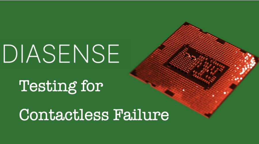
In Copenhagen, a startup called Diasense has been developing an instrument that seems, at first glance, almost anachronistic in its ambition. Rather than relying on ever sharper imaging, it seeks to detect failure indirectly, by listening for the faint magnetic signals generated by electrons moving through a chip’s circuitry. At the heart of the system is a quantum sensor, built from diamond, capable of measuring magnetic fields so small that they were once considered experimental curiosities rather than industrial tools.
The principle itself is not new. Physicists have long known that defects in solids reveal themselves through subtle disturbances in electromagnetic behaviour. What has changed, over the last decade, is the ability to measure those disturbances non‑invasively, at room temperature, and with sufficient spatial resolution to matter in chip fabrication. Diasense’s instrument uses nitrogen‑vacancy centres in diamond, atomic‑scale defects that behave as exquisitely sensitive quantum probes. When illuminated and interrogated with precision, these centres respond to local magnetic fields with measurable shifts that can be mapped into images.
The result is a microscope that does not show transistors as shapes, but as sources of activity. Instead of edges and layers, it reveals current paths, leakage points, and switching anomalies. Crucially, it does so without touching the chip, without coating it, and without cutting into it. The failure remains in situ, observed rather than disturbed.
This matters because modern chips are no longer planar objects. FinFETs, gate‑all‑around structures, stacked interconnects and buried power rails create three‑dimensional complexity that frustrates traditional inspection. A defect may be electrically active only under specific operational conditions, disappearing entirely when the chip is idle or cooled. Conventional microscopy freezes a device in time; quantum magnetic sensing observes it in action.
Diasense’s approach reflects a broader shift in semiconductor diagnostics, away from morphology and towards function. As devices approach atomic limits, the question is less what a transistor looks like than how it behaves under stress. Two transistors may be structurally identical but functionally divergent due to minute variations in dopant distribution, strain, or interface chemistry. These variations manifest electromagnetically, not optically.
The company’s insistence on describing its tool as a diagnostic platform rather than a microscope is telling. It suggests a reframing of failure itself. A faulty chip is no longer one that visibly deviates from design, but one that behaves unexpectedly in fields that were previously unobservable. Failure becomes probabilistic, contextual, and dynamic.
This reframing carries consequences. Yield loss in advanced manufacturing is increasingly driven by rare, hard‑to‑reproduce failures that evade conventional inspection. Engineers are forced to infer causes statistically, correlating large populations of chips with performance anomalies. A tool that can localise the physical origin of such anomalies, even after fabrication, could change the logic of process control. Instead of guessing where variation enters, manufacturers could observe it directly.
Yet restraint is warranted. Quantum microscopes are not panaceas. Their sensitivity is a double‑edged instrument. At atomic scales, noise is abundant. Distinguishing meaningful signals from benign fluctuation requires judgement as much as precision. There is also the question of integration. Semiconductor fabs are conservative environments, designed for throughput, reliability, and predictability. Introducing quantum sensors, however robust, demands new workflows and interpretive expertise.
Diasense’s engineers have been careful not to oversell. Their public descriptions focus on inspection and diagnostics rather than inline metrology. The instrument is positioned as a way to understand failure mechanisms, not necessarily to screen every chip. In this sense, it resembles an investigative tool more than a production one, closer to pathology than triage.
This distinction echoes earlier moments in the history of science. When microscopes first revealed bacteria, they did not immediately transform medicine; they first transformed understanding. The causal chain between observation and intervention had to be built slowly. Quantum magnetic microscopy may occupy a similar position in semiconductor technology.
It expands the space of what can be known before it dictates what must be done.
Denmark’s role in this story is not incidental. The country has cultivated a quiet competence in precision instrumentation and quantum sensing, often at the intersection of academic physics and applied engineering. Diasense emerged from this milieu, benefiting from long‑term research support rather than rapid commercial pressure. Its technology reflects that lineage: rigorous, careful, and oriented towards measurement as an end in itself.
The implications extend beyond chip manufacturing. Any technology that can non‑invasively detect electromagnetic anomalies at nanometre scales has potential applications in materials science, energy systems, and even biology. But it is in semiconductors, with their unforgiving tolerances and immense economic stakes, that the value proposition is clearest.
Invisible failures represent a peculiar crisis of modern engineering. Systems are failing not because they are badly designed, but because they are too finely tuned to tolerate uncertainty. As margins shrink, ignorance becomes expensive. Quantum microscopes offer not certainty, but visibility. They shine light, metaphorically, on processes that were once inferred only indirectly.
Whether this visibility will translate into fundamentally better chips remains an open question. What seems more certain is that it will change how engineers think about error. Failure is no longer simply something to eliminate; it is something to characterise, map, and perhaps even accept within narrower bounds. In that sense, quantum microscopes mark a shift not just in instrumentation, but in industrial epistemology.
The chip does not announce its flaws. It whispers them, in magnetic murmurs too soft for classical tools. Quantum microscopes exist to listen.
References
Barry, J. F., Turner, M. J., Schloss, J. M., Glenn, D. R., Song, Y., & Lukin, M. D. (2020). Optical magnetic detection of single‑electron spins. Proceedings of the National Academy of Sciences, 117(42), 26166–26174. https://doi.org/10.1073/pnas.2007847117
Diasense. (2026). Quantum diamond magnetic microscopy for semiconductor diagnostics. Company technical overview.
Degen, C. L., Reinhard, F., & Cappellaro, P. (2017). Quantum sensing. Reviews of Modern Physics, 89(3), 035002. https://doi.org/10.1103/RevModPhys.89.035002
Pop, E., Varshney, V., & Roy, A. K. (2012). Thermal properties of graphene: Fundamentals and applications. MRS Bulletin, 37(12), 1273–1281. https://doi.org/10.1557/mrs.2012.203
The Quantum Insider. (2026). Danish startup Diasense secures funding to scale quantum chip diagnostics.