At KTH Royal Institute of Technology in Stockholm, a newly inaugurated laboratory can deposit films only a few atomic layers thick and coat structures conventional methods struggle to reach. The facility strengthens Sweden’s capacity in quantum technology, photonics and energy materials, but its wider significance lies in a national attempt to turn expensive scientific instruments into shared industrial infrastructure.
A laboratory built around surfaces
Many important technological changes begin not with a new machine, but with a new surface.
A layer only a few nanometres thick can determine whether a semiconductor conducts or insulates, whether a solar cell captures light efficiently, whether a catalyst encourages the desired chemical reaction, or whether a superconducting component behaves predictably close to absolute zero.
Researchers at KTH Royal Institute of Technology now have a new instrument with which to design such surfaces almost one atomic layer at a time.
The recently inaugurated WISE Atomfab, located at Albanova Nanolab in Stockholm, combines advanced atomic layer deposition, or ALD, with chemical vapour deposition, usually abbreviated to CVD. The equipment allows researchers to produce extremely thin films and control their composition, thickness and structure with considerable precision.
The development was publicly announced by KTH on 24 September 2026. That date can be verified as the publication date of KTH’s Swedish- and English-language articles. The source describes the laboratory as “recently inaugurated”, but it does not provide a separate, exact inauguration date. WISE republished the announcement on 25 September. It would therefore be more accurate to say that the facility had been inaugurated by 24 September 2026, rather than to identify that date unequivocally as the opening ceremony itself.
It is also important to distinguish a new stand-alone institution from a new capability inside an established infrastructure. “Atomic-scale materials laboratory” is a serviceable description, but the official name used by KTH is WISE Atomfab. It forms part of Albanova Nanolab, rather than replacing or duplicating the nanolab. The significant new element is its advanced ALD equipment, accompanied by CVD capacity and integrated into a broader fabrication environment.
Atomic layer deposition
Atomic layer deposition is a vapour-phase technique based on a sequence of self-limiting surface reactions.
In a simplified process, a surface is exposed to one chemical precursor. Molecules react with available sites on that surface, but the reaction stops when those sites have been occupied. The system is purged, removing excess precursor and gaseous by-products. A second chemical is then introduced and reacts with the first layer. Another purge follows. Repeating this cycle gradually builds a film.
The thickness added during each cycle may be only a fraction of a nanometre. Because the reactions occur at the surface and are self-limiting, ALD can produce uniform, conformal and largely pinhole-free films. It can also coat recesses, sidewalls and complex three-dimensional structures that direct, line-of-sight deposition techniques may fail to cover evenly.
That ability is central to the KTH investment. Erik Holmgren, a researcher at the laboratory, gave the example of optical waveguides on which single-photon detectors could be positioned along the side or wrapped around part of a structure.
“This makes it possible to create new types of chips where thin films can be bent around corners,” he said in KTH’s announcement.
ALD should not be confused with the literal manual placement of individual atoms. The process relies on chemical reactions involving populations of molecules across a surface. Its “atomic” precision lies in its exceptionally fine control over growth, frequently approaching the thickness of an atomic layer per reaction cycle.
Nor is ALD automatically preferable to every other deposition method. Its cycles can make it slower than some competing processes, precursor chemistry can be difficult or expensive, and reaction temperatures must be compatible with the substrate. Residual impurities and incomplete reactions also have to be understood and controlled. Studies of ALD consequently combine surface chemistry, process engineering and extensive characterisation rather than relying upon the deposition instrument alone.
From funding to operational facility
The origins of WISE Atomfab extend beyond the 2026 announcement.
WISE, the Wallenberg Initiative Materials Science for Sustainability, was established as a national research programme financed by the Knut and Alice Wallenberg Foundation. It runs from 2022 to 2033 and has a total budget of approximately SEK 2.7 billion to almost SEK 3 billion, depending on whether the figure is stated precisely or rounded. Its declared purpose is to advance materials science that contributes to a sustainable society while educating researchers and strengthening collaboration between universities and industry.
In June 2023, WISE described plans to create national research infrastructures for advanced materials characterisation and fabrication. At that stage, it identified research facilities at Myfab and the MAX IV Laboratory as parts of a wider infrastructure effort with a stated budget of SEK 650 million.
In January 2024, the programme announced a SEK 500 million allocation specifically for equipment and infrastructure at seven Swedish universities. The intended platforms included electron microscopy, spectroscopy, crystallography, additive manufacturing and laboratories for the synthesis and fabrication of functional and circular materials. WISE initially expected much of the equipment to be commissioned during 2024 or 2025, although more complex platforms would require a longer build-up.
KTH was assigned responsibility for three platform areas. One was Materials Fabrication, intended to support two- and three-dimensional materials for electronics, photonics and energy conversion. The others concerned electron microscopy and high-field nuclear magnetic resonance and magnetic resonance imaging for materials research.
The Materials Fabrication platform is distributed between KTH and Lund University, with Vladislav Korenivski at KTH and Luke Hankin at Lund named as lead scientists. It comprises three complementary tools: combined ALD and CVD capacity at KTH, hot-wall metal-organic chemical vapour deposition at Lund and deep reactive-ion etching, also at Lund.
The logic is not merely to acquire three impressive machines. Lund’s equipment is intended to grow high-quality group III-nitride semiconductor materials and etch three-dimensional structures. KTH can then apply conformal coatings to complex forms using processes that are not constrained by line of sight. By November 2026, WISE described the KTH node as operational and inaugurated, while the Lund node was expected to become operational during 2027.
Publicly available sources do not disclose the manufacturer and model of KTH’s new ALD-CVD system, its purchase price, the procurement timetable, installation milestones or formal acceptance tests. Claims about those details would therefore require procurement records or direct confirmation from KTH. What the public record does establish is a progression from national infrastructure planning in 2023, through the platform funding decision in 2024, to an operational KTH installation in 2026.
Quantum materials only a few layers thick
Some of the laboratory’s most intriguing work may concern superconducting nitrides.
KTH says its researchers will use ALD to make superconducting, semiconducting and insulating materials for quantum technology. Making a material extremely thin can change its electrical and quantum-mechanical behaviour, creating properties that are weak, inaccessible or entirely absent in thicker films.
According to Erik Holmgren, chemical deposition provides control over film stress, density and crystallinity as well as thickness.
“When we can control virtually every atomic layer, we can produce thinner and more homogeneous films than before,” he said. “This is particularly interesting for quantum applications, where properties such as kinetic inductance are highly dependent on the thickness of the material.”.
Kinetic inductance arises from the inertia of charge carriers, and it can become especially pronounced in narrow or ultrathin superconducting structures. Reliable control of film thickness and homogeneity is therefore important in components such as sensitive photon detectors, resonators and other superconducting circuits.
Yet the laboratory should not be characterised solely as a quantum facility. KTH identifies possible uses in photonics, solar-energy conversion, catalysis and pharmaceutical manufacturing. More broadly, ALD is used or investigated in microelectronics, batteries, energy storage, membranes, medical surfaces and advanced nanopatterning.
These diverse applications share a requirement for controlled interfaces. A material’s surface can determine how it exchanges electrons, light, ions, heat or molecules with its surroundings. The capacity to alter that boundary without redesigning the entire bulk material is one reason thin-film engineering has become strategically important.
An open laboratory, not an isolated machine
WISE Atomfab is intended as shared research infrastructure. KTH says it is open to external researchers through Myfab and the Nordic Nanolab Network. Researchers from Stockholm University, Karolinska Institute, regional start-ups and industry are among its prospective or existing user communities.
Adrian Iovan, who works at the laboratory, described it as “small but efficient”, while acknowledging that more potential users needed to be made aware of its existence.
That point is more significant than it may appear. A sophisticated deposition system produces little public value if it lacks trained operators, reliable process recipes, maintenance budgets, characterisation tools or a practical access mechanism. The ability to make a film is only the beginning. Researchers must establish what was deposited, how uniform it is, whether it contains defects or impurities and how its properties change when integrated into a device.
Albanova Nanolab already sits within Myfab, Sweden’s national infrastructure for micro- and nanofabrication. The network links cleanrooms at KTH, Chalmers University of Technology, Lund University and Uppsala University. According to Chalmers, the network provides more than 750 processing and characterisation tools, employs 89 expert staff and serves 877 active users, including 120 companies.
KTH’s infrastructure register confirms that external use of Albanova Nanolab is fee-based and that pricing is aligned with Myfab’s model. In other words, Atomfab is not simply a university laboratory carrying out internally selected projects. It forms part of a user infrastructure in which academic and commercial customers can apply for access, receive training and book equipment.
A Nordic strength, not a Nordic monopoly
KTH’s installation is noteworthy, but it does not place Stockholm alone at the summit of Nordic ALD research.
Finland has a particularly deep history in atomic layer processing. ALD Center Finland at the University of Helsinki is a national, open-access platform for atomic layer deposition and atomic layer etching. It combines reactors for process and precursor development with in-situ and in-vacuum analytical methods designed to reveal the chemistry occurring during deposition.
The centre reports 12 smaller ALD and atomic-layer-etching tools in addition to its cluster system, including reactors accommodating wafers of up to 150 or 200 millimetres. Its researchers have experience with hundreds of ALD processes.
In Espoo, Micronova, jointly operated by Aalto University and VTT Technical Research Centre of Finland, comprises 2,600 square metres of cleanroom space and more than 380 tools. It combines university nanofabrication, ALD process development and industrially orientated pilot production, including processing for wafers up to 200 millimetres.
Sweden also possesses mature fabrication environments beyond KTH. Myfab Chalmers, for example, operates a 1,240-square-metre cleanroom with electron-beam lithography, thin-film deposition, plasma processing and semiconductor-growth capabilities.
The proper comparison, therefore, is not between a previously empty Nordic landscape and one new Swedish machine. It is between complementary facilities. Helsinki has unusual strength in ALD chemistry, precursors and reaction mechanisms. Micronova connects fabrication research with pilot-scale processes. Chalmers offers an extensive device-fabrication environment. The KTH-Lund platform contributes a deliberately linked chain of materials growth, three-dimensional etching and conformal deposition.
In research infrastructure, distinction frequently lies in the combination of instruments, processes and expertise rather than in ownership of a technique that no one else possesses.
From scientific capability to industrial value
The industrial argument for WISE Atomfab rests on access and translation. Start-ups and established companies often require only a limited number of experimental wafers or samples during development. Buying an ALD system, installing gas-handling and abatement equipment, maintaining a cleanroom and employing specialist process staff can be beyond the reach of a young company. Shared facilities allow such firms to test whether a material or coating works before committing to their own production line.
This model can shorten the distance between a university experiment and a manufacturable component. It may also reduce duplication, provided that access arrangements, intellectual-property rules and waiting times remain workable.
The risks are equally clear. Research equipment can become fragmented across institutions; process recipes may not transfer smoothly from experimental samples to industrial wafers; and a coating demonstrated in a laboratory may prove too slow, expensive or chemically demanding for volume manufacture. Small research infrastructures can also become dependent on a few specialists whose departure would remove much of the facility’s practical competence.
Evidence of success should consequently extend beyond the number of deposited samples. Over the next few years, more revealing measurements will include external-user numbers, industrial projects, uptime, reproducible material processes, peer-reviewed research, patents, start-ups and devices that progress into pilot manufacturing.
Precision as infrastructure
The importance of WISE Atomfab does not lie in the theatrical notion of scientists stacking atoms like bricks. It lies in the less visible discipline of controlling surfaces, interfaces and imperfections.
The laboratory gives researchers at KTH and elsewhere a more versatile means of coating three-dimensional structures and making ultrathin superconducting, semiconducting and insulating materials. Its connection to Lund’s forthcoming equipment, the wider Myfab network and WISE’s national platforms makes it part of a distributed system rather than an isolated institutional acquisition.
Whether that system produces sustainable technology will depend on choices made after the inauguration: which materials are prioritised, how environmental trade-offs are assessed, whether companies can gain effective access and whether promising processes can move beyond single samples.
The new laboratory does not, by itself, deliver a quantum computer, a more efficient solar cell or a cleaner industrial catalyst. It supplies something more fundamental: a place where researchers can determine, one vanishingly thin layer at a time, whether such technologies can be made to work.
References
Aalto University. (2026). Micronova. [aalto.fi]
Chalmers University of Technology. (2026). Myfab Sweden. [chalmers.se]
Chalmers University of Technology. (2023). Myfab Chalmers facility. [chalmers.se]
Kessels, E., Devi, A., Park, J.-S., Ritala, M., Yanguas-Gil, A., & Wiemer, C. (2025). Atomic layer deposition. Nature Reviews Methods Primers. [nature.com]
KTH Royal Institute of Technology. (2024, January 12). KTH part of major Swedish investment in materials research. [kth.se]
KTH Royal Institute of Technology. (2026, September 24). New lab for building materials at the atomic scale. [kth.se]
KTH Royal Institute of Technology. (2026). KTH research infrastructures. [kth.se]
Oviroh, P. O., Akbarzadeh, R., Pan, D., Coetzee, R. A. M., & Jen, T.-C. (2019). New development of atomic layer deposition: Processes, methods and applications. Science and Technology of Advanced Materials, 20(1), 465–496. [pmc.ncbi.nlm.nih.gov]
Shahmohammadi, M., Mukherjee, R., Sukotjo, C., Diwekar, U. M., & Takoudis, C. G. (2022). Recent advances in theoretical development of thermal atomic layer deposition: A review. Nanomaterials, 12(5), 831. [pmc.ncbi.nlm.nih.gov]
University of Helsinki. (n.d.). ALD Center Finland. [helsinki.fi]
University of Helsinki. (n.d.). ALD/ALEt reactors. [helsinki.fi]
WISE. (2023, June 29). WISE establishes national research infrastructure. [wise-materials.org]
WISE. (2024, January 12). WISE invests in research and technology platforms. [wise-materials.org]
WISE. (2026). Materials Fabrication. [wise-materials.org]
WISE. (2026, September 25). New lab for building materials at the atomic scale. [wise-materials.org]
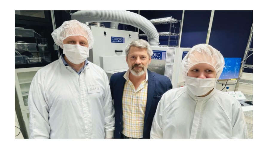
Photo: Four crucial components for the new Atomfab: Adrian Iovan, Vladislav Korenivski, Erik Holmgren and the ALD financed by WISE (Wallenberg Initiative Materials Science for Sustainability).