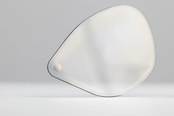
The quest to make electronics both smaller and cleaner has often been told through the lens of chip fabs and ever‑shrinking transistor gates. But a quieter revolution is unfolding in the Nordics, where researchers are using printing, not photolithography, to pattern metals, dielectrics and semiconductors with features measured in micrometres and, increasingly, below. At the centre of this story is VTT in Finland, which has demonstrated one‑micrometre accuracy using reverse‑offset printing, a milestone that redraws the boundary between additive manufacturing and the long‑dominant cleanroom paradigm.
The proposition sounds simple: borrow the speed, scalability and low‑waste ethos of the graphics industry and apply it to functional electronics. What kept printed electronics on the periphery for years was resolution, overlay alignment and materials performance. One‑micrometre lines and micrometre‑scale overlay open an entirely different class of devices—fine metal meshes for transparent conductors, antennae and RF circuits, high‑density sensor arrays, metasurfaces, and even elements of display backplanes, without the capital intensity or environmental footprint of vacuum processing. VTT states that its reverse‑offset system reaches 1 μm line features and μm‑level alignment, positioning the method for roll‑to‑roll scale and applications from touch panels to metamaterial surfaces; it’s an advance they argue can ease component shortages while offering more sustainable manufacturing routes.
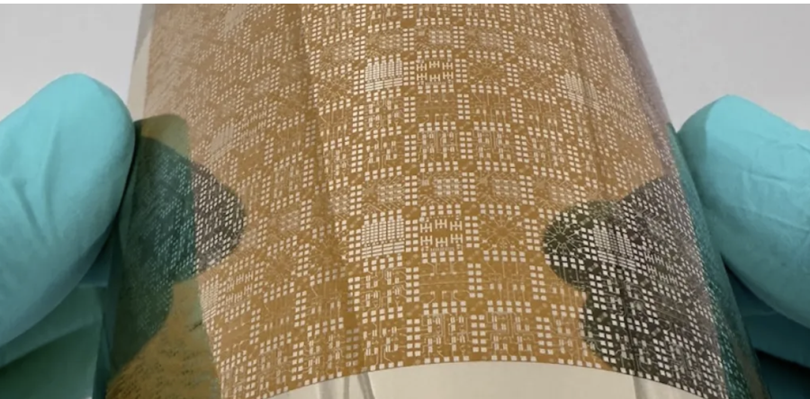
Reverse‑offset printing (ROP) is the enabling mechanism. Unlike direct wet printing, ROP prepares the ink into a semi‑dry state on a compliant PDMS roller; the roller contacts a relief plate (the cliché) that lifts away unwanted regions before transferring the patterned, semi‑dried ink onto the final substrate. This sequence helps defeat typical wetting and spreading limits and yields exceptionally fine, well‑defined edges. Independent analysis from TechBlick underscores the point, highlighting VTT’s example with silver nanoparticle inks achieving 1 μm lines, typical ROP minimum resolutions in the 0.5–5 μm range, overlay accuracy better than ~2 μm, and practical printing speeds on the order of metres per minute, performance that begins to “encroach into the realm of photolithography.”.
The groundwork in Finland goes back several years. VTT researchers reported roll‑to‑roll ROP achieving one‑micrometre resolution with homogeneous line edges as early as 2018 in Flexible and Printed Electronics. That peer‑reviewed study examined the critical interactions among nanoparticle inks, plastic substrates, PDMS blankets and nickel stamps, exactly the messy interfacial science that determines whether micrometre lines come out crisp, conductive and repeatable. In parallel, VTT engineers described “taking the accuracy beyond 1 μm” in trade‑press and conference outlets, evangelising the method’s potential for RF circuits and miniaturised systems where printed electronics previously struggled to compete.
The SYNERGY project, where VTT is a partner, amplified the message to Europe’s materials‑and‑devices community, showcasing sub‑micrometre lines and μm‑scale alignment as a new baseline rather than a lab curiosity. A short VTT video circulated via SYNERGY captured the micro‑patterning steps and linked them explicitly to the environmental dividend: less material, lower energy and a path to recyclable or biodegradable substrates.
What distinguishes the Nordic push is not only the device resolution but the process architecture. A 2021 VTT‑authored paper in ACS Applied Materials & Interfaces showed a hybrid lift‑off approach: print a sacrificial polymer resist via ROP at micrometre scale, deposit metals/oxides by vacuum, then lift off. The result was sharp, low‑roughness sidewalls in aluminium, ITO and dielectrics, enabling transparent metal‑mesh conductors and thin‑film transistor electrodes with printed origins and linewidths down to ~1 μm. It is a pragmatic bridge between additive and subtractive, combining the best of both worlds while keeping temperatures and costs in check.
Across the Atlantic and in Asia, the race to sub‑micrometre printed features is accelerating, an important backdrop when assessing Nordic leadership. Duke University’s team, working with Hummink Technologies, has demonstrated “high‑precision capillary printing” of fully recyclable carbon‑based thin‑film transistors at sub‑micrometre scales, with the express aim of transforming display backplanes and reducing the sector’s energy and emissions footprint. The method prints features with gaps smaller than a micrometre using a vibrating micro‑pipette and capillary forces, another route toward the same endgame of high‑density, lower‑impact manufacturing. The work, published in Nature Electronics, positions recyclable inks and precision additive patterning as credible alternatives to conventional vacuum TFT lines for large‑area displays.
Against this global canvas, the Nordic edge is strategic. The VTT platform doesn’t sit in isolation; it connects to European programmes focused on micrometre‑scale printed OLAE (organic large‑area electronics). The EU‑funded HI‑ACCURACY project set explicit targets for front‑ and backplane structures with feature sizes approaching 1 μm, leveraging low‑temperature curable nano‑Ag/Au conductors and advanced printable semiconductors, an ecosystem where VTT has been an active partner alongside Fraunhofer, JOANNEUM and others. By designing for manufacturability from the outset (including barrier stacks and multilayer integration), these initiatives aim at TRL‑5 demonstrators suitable for industrial validation, particularly in displays.
The implications for metamaterials and photonics are especially compelling for a Nordic region with strengths in radio, radar and optical systems. One‑micrometre‑class lines and μm‑scale overlay accuracy enable periodic structures with sub‑wavelength control across large areas—think metasurfaces that manipulate electromagnetic waves for beam steering, radar cross‑section shaping or colour without pigments. VTT has explicitly signposted metamaterial surfaces, long‑range directional radio links and radar reflectors as near‑term application classes for its reverse‑offset capability, areas with clear dual‑use relevance for both civil infrastructure and defence.
There is also a sustainability narrative that resonates with Nordic industrial policy: printing is inherently parsimonious with materials, and ROP’s semi‑dry transfer minimises solvents at the point of patterning. VTT’s communications emphasise reduced energy and material inputs, the possibility of biodegradable substrates, and the prospect of alleviating component supply bottlenecks by localising production in modular, roll‑to‑roll lines rather than capital‑heavy fabs. In an era of strategic autonomy and supply‑chain risk, that matters.
Technically, the open questions are precisely the ones a Nordic RTO is structured to attack: multi‑layer registration at speed; sheet resistance versus transparency trade‑offs in sub‑micrometre metal meshes; low‑temperature sintering compatible with plastics; and the lifetime stability of conductive and semiconductive prints under thermal and humidity cycling. The TechBlick analysis, for example, called out the relatively high sheet resistance (~100 Ω/□) for very thin 1 μm silver lines on PET; acceptable for many sensor and EMI applications, but demanding optimisation when targeting display backplanes or power distribution. This is where materials innovation, switching to copper with robust anti‑oxidation chemistries, hybrid inks, or stacked conductor architectures, enters the frame, and where Europe’s inks‑and‑materials community is already active.
If the technical path is credible, the intellectual‑property terrain must be navigated carefully. Reverse‑offset as a concept is not new; prior art exists in Korea and elsewhere, such as a KIMM‑assigned US patent describing a “partial‑off” reverse‑offset method with PDMS blankets and clichés for functional inks. For Nordic actors, the operative task is to fence off process refinements, ink rheologies for semi‑dry transfer, cliché designs, blanket chemistries, multi‑pass overlay strategies and roll‑to‑roll control that translate into yield and reliability advantages at 1 μm and below. That is where freedom‑to‑operate can be maintained while building a defensible moat.
What would a distinctly Nordic roadmap look like from here? First, lean into domains where micrometre features unlock value at scale: transparent conductors for AR/VR optics and automotive HUDs; antenna arrays for sub‑6 GHz and mmWave comms; biosensor electrodes with high surface‑to‑volume ratios; and metasurfaces for radar and satellite links, areas with immediate regional industrial pull. VTT’s own framing (displays, metamaterials, touchscreens, PV cells and biosensors) is a credible short‑list that plays to regional strengths in photonics, wireless and green tech. Second, formalise roll‑to‑roll demonstration lines with industrial partners to derisk yield, overlay and uptime over multi‑kilometre runs; this is the bridge from lab hero numbers to production contracts and exportable machines. The 2018 roll‑to‑roll ROP paper is the DNA of that transition; by codifying process windows and interfacial controls, it gives machine builders and materials suppliers a starting point for spec sheets rather than a slide deck of possibilities. Third, integrate hybrid lift‑off (printed resist + vacuum deposition) where outright printed material performance still lags, a path VTT has already validated for metals and oxides.
The global comparator set is robust. Japan has long led in high‑resolution printing for OTFTs, with reverse‑offset‑fabricated organic inverters achieving sub‑3 μm channel lengths several years ago, evidence that precision additive patterning can deliver functional logic at low voltages when materials and patterning co‑evolve. Korea’s early patent work and industrial machine development show a sustained commitment to reverse‑offset processes in display and sensor supply chains. Meanwhile, the U.S. is mobilising around the recyclability and energy‑efficiency angle, as the Duke‑Hummink results make clear, tying sub‑micrometre printing to reshoring ambitions. The opportunity for the Nordics is to occupy the sweet spot where high‑precision printing meets sustainability, open innovation and manufacturability, fields that favour coordinated public–private action and strong RTOs.
There is a cultural fit here, too. Nordic industry is comfortable with platform plays—shared infrastructure, common materials stacks, interoperable pilot lines because that is how small markets create global leverage. VTT’s own posture as “R&D partner in sustainable growth,” with deep piloting capability and a track record of spin‑offs and ecosystem building, is a case in point. When a technology sits between disciplines (printing, materials science, RF design, optics), that orchestration capability becomes a competitive advantage in its own right.
Sceptics may argue that micrometre isn’t nanometre, and that photolithography will remain unassailable for silicon logic. Both statements are true and irrelevant to where the growth and environmental impact are in large‑area electronics. The displays that dominate our surfaces, the sensors that populate our supply chains, the antennas that knit our networks and the metasurfaces that will reshape our interaction with electromagnetic fields: these are applications where designable conductors and dielectrics at 1 μm, placed rapidly and cheaply over large areas, deliver both performance and decarbonisation. The question is not whether printed electronics will replace fabs; it is how quickly we can widen the envelope where printing is the rational choice.
On that measure, the Nordic story is already persuasive. In a field prone to PowerPoint promises, VTT has put steel and silicone on the floor: a reverse‑offset platform with one‑micrometre resolution, proven overlay, and a line‑of‑sight to roll‑to‑roll production and system‑level demonstrators in displays, photonics and RF. The rest is execution and tight integration with European materials leaders, industrial‑scale reliability data, and a pipeline of lighthouse applications that make the benefits visible on the streets of Helsinki, Oulu and beyond. For a region that wants to build prosperity on clean manufacturing rather than just clean aspirations, one‑micrometre is not merely a number. It is a threshold that, once crossed, turns printing from a curiosity into a contender.
SourcesVTT, “Printed electronics reaching accuracy of one micrometre” — overview of reverse‑offset capabilities and applications. Link [vttresearch.com]
- TechBlick, “Taking the accuracy of printed electronics below 1um” — technical explainer of ROP process and performance metrics. Link [techblick.com]
- SYNERGY project, “Printed electronics reaching accuracy of one micrometre by VTT” — project note and video reference. Link [synergyproject.eu]
- Sneck, Mäkelä, Alastalo, “Reverse‑offset for roll‑to‑roll high‑resolution printing,” Flexible and Printed Electronics (2018). Link [cris.vtt.fi]
- Sneck et al., “Reverse‑Offset Printing of Polymer Resist Ink for Micrometer‑Level Patterning of Metal and Metal‑Oxide Layers,” ACS Applied Materials & Interfaces (2021). PDF [pubs.acs.org]
- Alastalo, “Taking the accuracy of printed electronics beyond 1 μm,” OPE Journal (overview). Link[academia.edu]
- VTT video, “Printed electronics reaching accuracy of one micrometre at VTT” (YouTube). Link [youtube.com]
- HI‑ACCURACY (H2020) project fact sheet (CORDIS). Link [cordis.europa.eu]
- VTT project page for HI‑ACCURACY. Link [cris.vtt.fi]
- Duke University / Pratt School of Engineering — sub‑micrometre recyclable printed electronics announcement and context. Link [pratt.duke.edu]
- EurekAlert! press release on Duke/Hummink high‑precision capillary printing. Link [eurekalert.org]
- Tech Xplore coverage of Duke work (PDF mirror). Link [techxplore.com]
- Google Patents: US20130255519A1 “Reverse offset printing method of partial off type” (KIMM). Link[patents.google.com]
- VTT corporate overview and partner model (for ecosystem context). Link [vttresearch.com]
- Background comparator (Japan): reverse‑offset printed organic TFT inverters (contextual reading). Link[advanced.o….wiley.com]