Finland’s position as a rising force in microelectronics and photonics is exemplified by the collaboration between Dispelix, a leading developer of augmented reality (AR) waveguides, and VTT, whose shared-use cleanroom at Micronova provides the advanced infrastructure required for next‑generation optical manufacturing. The partnership demonstrates how shared national capabilities can accelerate deep‑tech innovation while strengthening Europe’s strategic autonomy in semiconductor‑adjacent technologies.
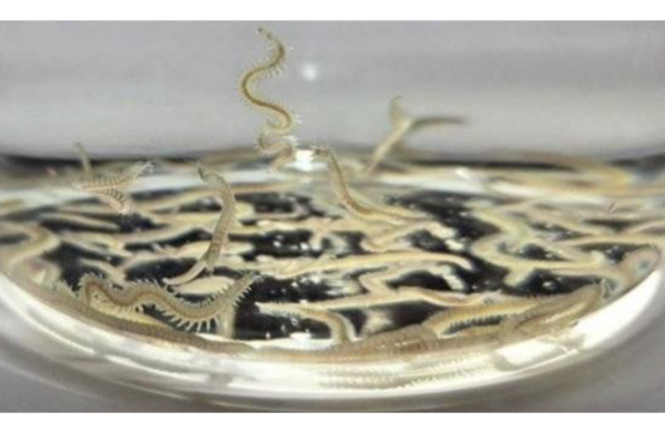
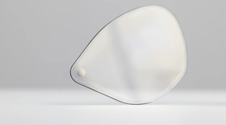
Founded in 2015 as a VTT spinoff, Dispelix designs and manufactures transparent waveguides—ultra‑thin optical elements that act as see‑through displays for AR devices. These components rely on nanoscale gratings, typically only 200–300 nanometres in size, to guide light through a glass substrate using total internal reflection. Producing such structures requires exceptionally clean, stable and precise fabrication environments—conditions that would be prohibitively expensive for most companies to build independently.
VTT’s shared-use cleanroom model, unique in Europe, gives Dispelix flexible access to industrial‑grade microfabrication tools, expert maintenance and a controlled environment suitable for both early‑stage R&D and pilot‑scale production. According to Joonas Heikkinen, Cleanroom Operations Director at Dispelix, the ability to work directly inside the cleanroom is essential: “Waveguide development demands an environment where every source of interference is removed. A single dust particle can ruin the final optical performance.”
Because Dispelix works primarily with glass rather than silicon, its processes differ significantly from standard semiconductor workflows. The hybrid operating model at Micronova allows Dispelix engineers to run their own specialised processes while also training VTT operators to support specific steps when needed. This flexibility provides scalability without the need for large in‑house staffing or capital expenditure. Building even a fraction of the required infrastructure independently would cost tens of millions of euros.
VTT’s continuous investment in microfabrication capabilities further strengthens this collaboration. In 2025, the cleanroom was upgraded from 150 mm to 200 mm wafer compatibility, aligning it with other leading European R&D facilities and improving tool performance and process stability. “Our goal is to build a leading European microelectronics R&D and piloting cleanroom,” says Piia Konstari, VTT’s Director of Microfabrication Services. “This investment strengthens Finland’s role in the specialised microelectronics ecosystem.”
The benefits extend beyond Dispelix. By opening its cleanroom to startups, spinoffs, research groups and industrial partners, VTT supports a growing cluster of microelectronics and photonics expertise. This momentum is set to accelerate further through Kvanttinova, a new joint initiative by VTT, Aalto University, the City of Espoo and industry partners. The hub will expand Finland’s capabilities across microelectronics, photonics and quantum technologies, creating a concentrated environment for innovation.
Heikkinen sees Kvanttinova as a catalyst for ecosystem growth: “When companies, researchers and new capabilities concentrate in one place, the whole ecosystem becomes more attractive—for talent, for investment and for collaboration.” Aalto University’s presence is particularly valuable for early experimentation and small‑scale testing, complementing VTT’s industrialisation‑focused environment.
For Dispelix, this combination of shared infrastructure, academic collaboration and industrial‑grade capabilities provides a development pathway that would be extremely difficult to replicate elsewhere. It also reinforces Finland’s position as a global leader in AR optics and advanced microfabrication—an achievement built on strategic cooperation, shared resources and a commitment to deep‑tech excellence.